| Česky | English |
Charles University in Prague,
Faculty of Mathematics and Physics, Department of Electronics and Vacuum
Physics
Thin Films Group
|
Gallery STM in-vivo
Adsorption and mobility of Ag atoms on the surface Si(111)7x7 (AVI, 1.9 MB)
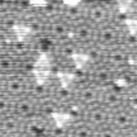 |
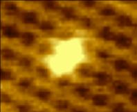
Surface of a silicon mono-crystal - a plane (111) with 7x7 reconstruction is composed by large (2.7 nm) triangular half unit cells (HUCs) of two various types - faulted (FHUCs) and unfaulted (UHUCs) - containing 6 Si adatoms each. Neighboring HUCs are different, deposited Ag atoms spend more time in FHUCs. The Ag atoms are bounded at various surface positions, they can easily hop among the adsorption positions within a HUC at room temperature, but inter-cell hops are less frequent and corresponding energy barriers are higher. The energy for hops of Ag atoms is provided by thermal vibrations of Si substrate atoms. Resulting random migration of Ag atoms along the surface represents two dimensional brownian motion. Due to relatively small speed of a scanning STM tip with respect to the fast motion of an Ag atom occupying a HUC the presence of the Ag atom in a HUC is indicated by highlighting corner Si adatoms in the HUC. The sequence of STM images shows inter-cell hopping of Ag atoms at surface temperature of 310 K, a time period between images is 1 min, the whole sequence duration is 170 min. The "film" shows formation and decay of a dimer (two Ag atoms in a HUC). An analysis of sequences taken at various temperatures allowed to specify microscopic parameters of the inter-cell hopping. |
Initial stages of heteroepitaxial
growth of Ag on Si(111)7x7 (WMV, 2.4 MB)
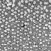 |
The sequence of STM images obtained during the deposition of Ag on the silicon surface at room temperature. Such an experiment is possible by using an extremely sharp STM tip to limit a screening effect of the tip during deposition on a scanned surface area. The images show that single Ag atoms rest in HUCs where they arrived until the moment when a dimer or a cluster containing >2 Ag atoms appears in an adjacent HUC. Such an object considerably affects the inter-cell mobility of single Ag atoms in neighborhood and growth regime dramatically changes. The film shows the growth on the surface area of 36 nm x 36 nm within 120 min at a rate 1 image/min and a deposition rate of 3x10⁻⁵ monolayer/s. |
Heteroepitaxial growth of Ag on the surface Si(100)2x1 (AVI, 12.2
MB)
 |
Direct observation of deposition of Ag atoms on surface of silicon mono-crystal - planes (100) with the 2x1 reconstruction. The reconstruction consists of Si dimer rows which are imaged as light strips. Si dimers are perpendicular to the row direction. Two directions of the dimer rows alternates - perpendicular or parallel with step edges of atomic terraces. Shape of growing two dimensional Ag islands is determined by the surface reconstruction. Ag atoms are arranged in dimer rows as well but Ag dimers are parallel to the direction of the Ag row. The Ag rows growth perpendicular to the dimer rows of the silicon surface reconstruction. The size of the imaged area is 80 nm x 80 nm, the image sequence shows high mobility of Ag atoms (fast Ag atoms cannot be identified by "slow" STM scanning) and the islands at room temperature. The period between images of the sequence is 110 s. The dimer rows represent a natural raster with a period of about 0.8 nm. |
Growing indium atomic chains at deposition on the surface Si(100)2x1 (avi, 4.21 MB)
 |
STM imaging during deposition of In on the silicon surface at room temperature. The surface mobility of particular indium adatoms is very high at room temperature and cannot be recorded by means of “slow” STM until two atoms meet and form a dimer – a stable immobile object. The indium dimers are parallel to the silicon dimers i.e. perpendicular to the silicon dimer rows of the surface reconstruction and lay between them. Further In adatom binds to the surface behind a free termination of an In dimer or joins an already bound adatom and forms another dimer. Such a mechanism results in growing straight metal chains composed by the dimers. An In adatom is bound by two bonds to Si atoms of two neighbouring dimers and the third one binds the other In adatom in a dimer or remains "dangling". If the atomic chain terminates by a single unpaired adatom, its unsaturated electron orbital (dangling bond) protrudes from the surface and is imaged as a bright "flag" at the chain termination. It is an image artefact due to an insufficient response of STM back-loop on abrupt change in charge density above the surface at fast scanning (scanning direction from right to left). The "flags" indicate single atom terminations of the indium chains in filled states images. ( Us=-2V, It=0.3 nA, deposition time about 60 min) |
Indium adatom hopping on the surface Si(100) at 78 K (avi, 10.6 MB)
 |
Single adatom imaging at low temperature.
Indium adatoms spontaneously hop among adsorption sites. It is thermally activated movement – the rate of hopping decreases with the lowering temperature, especially between sites separated by higher energy barriers. At a temperature of 78 K an indium adatom is imaged as a bright "cloud" because it does not rest at the same adsorption site during the scanning. The atom circulates among four very close sites – local minima of bonding energy potential surface – separated by barriers of about 0.2 eV. The hopping can be thermally activated or the energy for hopping can be provided by tunnelling electrons as well. Multiple recording of a fast hopping adatom in the whole area of the local minima results in imaging in a form of the bright "cloud". |
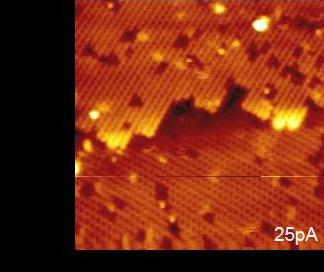 |
Larger distance hops of indium adatoms – into an area of the four neighbouring adsorption minima – need more energy and are less frequent. They are recorded in a sequence of STM images as hops of the "clouds" at the temperature of 78 K. An activation by the tunnelling current is not negligible – while at the tunnelling current of 25 pA single hops can be distinguished (see the first 31 frames of the sequence) increasing the current to 100 pA accelerates the adatom mobility enough to be imaged in the movement as "fuzzy" objects – composed by several bright lines. Note a thermal drift during the recording the sequence of 41 images with a rate of 60s/image. Filled state images (Us=-1.8 V), size of imaged area: 25 nm x 25 nm. |